Thin films are one of the most widely used classes of nanomaterials with applications in semiconductors, optics, flexible electronics, and functionalized surfaces for architectural glass – where a manufacturer may regularly deposit films with of only a few nanometers in thickness over square kilometers of area! To ensure quality over large areas, testing needs to be rapid and accurate. Nanoindentation testing with continuous stiffness measurement (CSM) provides a rapid, local method for investigating the mechanical behavior of thin films. In this application note, nanoindentation measurements are successfully demonstrated on two different thin films with thicknesses of 100 and 550 nm.
Introduction
The indentation of thin films and coatings was one of the original motivations for the development of nanoindentation [1]. The ability to accurately evaluate the properties of sub-micron scale thin films is essential for a wide variety of industries from machine tools to semiconductors. However, the measurement of the mechanical behavior of materials at such small length scales required some significant advances in both sensors and measurement electronics. Servo hydraulic actuators and linear variable differential transformer (LVDT) sensors used for macro-scale testing lacked the precision necessary to characterize thin films. Early nanoindentation systems used a voice-coil actuator, similar to a loudspeaker, for load actuation and capacitance-based displacement sensors. Current systems used high-precision MEMS-based load sensors and piezo-scanners to perform displacement-controlled indentations with high-performance dynamics.
However, the main challenge of thin film nanoindentation is not simply the performance of the indentation at small scales, it is the analysis of the resulting data. A nanoindentation measures both the elastic and plastic properties of the material underneath the indentation, but in thin film nanoindentation there are not one but two materials involved: the thin film and the substrate. Thus, the elastic and plastic strain fields underneath the indentation frequently encounter both materials, causing a mixed response. For the plastic strain field, the size of the plastic zone is usually on a similar scale to the width of the indentation, implying that an indentation needs to be ~10× shallower than the coating thickness for the measured hardness to be unaffected by the substrate properties. The elastic strain field is much larger than the plastic zone, so the indentation would need to be even smaller. For thin films with thicknesses less than a few tens of nanometers, this criterion quickly requires indentations on the scale of single nanometers.
So how do we meet this challenge? In this application note, we demonstrate the advantages of using continuous stiffness measurement nanoindentation [2] for the characterization of thin films and coatings. Two Aluminum thin films of different thickness are measured using both simple and CSM indentation methods. The results are compared and discussed in the context of the ISO standard on the nanoindentation of thin films [3].
Experimental Considerations
For a system to perform this application, two factors are important to remember: the system’s resolution and it’s CSM capability. As stated in the previous section, high-resolution sensing is essential for measurements on thin films. However, the ability to dynamically measure the evolution of hardness and elastic modulus with penetration depth also offers many advantages. In this section, we discuss these and the experimental procedures followed in this application note.
Continuous Stiffness Measurement
Indentation testing is typically performed in one of three ways: simple monotonic (SI), load/unload (LU), and continuous stiffness measurement (CSM). In the first, the load/displacement is applied in one continuous cycle. In the second, the load/displacement is applied incrementally in multiple stages with some degree of unloading in between stages. In the last, the load or displacement is applied with a dynamic sinus wave superimposed on the main load/unload cycle. This is usually achieved using a lock-in amplifier to maintain a CSM displacement amplitude of ~2 nm.
One can think of CSM indentation as an evolution of multiple load/unload cycles to the maximum number of cycles possible within the dynamics of the instrument, i.e. load/unloading as fast as the instrument can while avoiding system resonances.
This has several benefits for the user: more data vs depth, greater location specificity, and higher speed. This is illustrated in Figure 1, where the load-displacement curves and resulting hardness and reduced elastic modulus are shown as a function of contact depth.
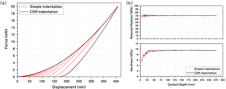 Figure 1. (a) Force-displacement curves for Berkovich indentations on fused silica and (b) resulting hardness and reduced modulus vs contact depth from both simple and CSM indentations.
This illustrates the difference in results from a single CSM indentation (1000s of datapoints per indentation) and 80 simple indentations (20 datapoints with std. deviation). However, good agreement is observed between the values from the two different methods.
Further, the time difference between these measurements is significant, as each CSM indentation takes ~90 seconds, which yields more data than the 80 simple indentations performed in two hours. While the difference in statistical significance could be discussed at length, the increase in measurement speed is still over an order of magnitude.
Since the same amount of information is effectively acquired from a single indentation, this also provides great benefits in terms of lateral resolution or area investigated on the material. Similar data can be extracted from a single location, which removes the influence of any variation in the material with location from the measurement as a function of depth. It also allows for the variation over large areas to be much more quickly investigated.
Experimental Procedures
Thin Aluminum films were directly deposited on a (100)-oriented Silicon wafer using a commercial magnetron sputtering system (PVD Products Inc.). The sputtering was carried out in DC mode with an Ar pressure of 3 mTorr and a flow rate of 50 sccm. The power was kept at 250 W for Al (99.99% MSE Supplies). The base pressure was kept below Torr and the substrate temperature was kept lower than 30 °C during deposition. The substrate was rotated at 30 rpm to obtain a uniform thickness of the deposited layer. The thickness of the Al films was controlled by varying the deposition time.
Nanoindentation testing was performed using an i04 Femto-Indenter with a FT-S20,000 sensor fitted with a Berkovich diamond tip. Simple indentations were performed using a constant ramp time with a logarithmic variation in maximum load (20–20000 µN) to produce indentations to a range of different depths. A loading ramp time of 50 s with a 20 s hold on unloading was used. For simple indentations in fused silica, shown in Figure 1, 4 indentations were performed at each of the 20 different load targets, and for the aluminum thin films it was 4 indents for each of 10 different load targets.
CSM indentations were performed in displacement control at a rate of 10 nm/s and an oscillation amplitude of 2 nm. A minimum of 6 indentations were performed for each coating with each indentation taking 90 seconds.
Electron micrographs were taken using a Zeiss EVO 25 SEM at an acceleration voltage of 10 kV with an Everhard-Thornley detector for secondary electrons (SE) and a HD Backscattered Electron Detector (BSE).
Results and Discussion
Two different films were investigated in this application note. Each was indented using both monotonic, simple indentation and dynamic, CSM indentation methods to various depths. The results of these indentation are shown in Figure 2.
As with the fused silica in Figure 1, the values from both simple indentation and CSM indentation show good agreement. The hardness values at lower contact depths show a slight increasing trend or a plateau before increasing more rapidly as a function of depth at higher depths. This initial region of the data is dominated by the intrinsic properties of the coating, while values at higher depths correspond more to the substrate’s properties.
Reduced modulus values show a related, but different trend in behavior. The values at higher depths plateau near the reduced modulus of the substrate silicon (160 GPa – [4]), while the values at lower depths more rapidly decrease with decreasing depths towards the value for the reduced modulus of Aluminum (75 GPa – [5]). This demonstrates the greater size of the elastic deformation field underneath the indenter, and thus the greater effect of the substrate on the measurement of the modulus.
When we compare the behavior of these two coatings in Figure 2, we can see that the reduced moduli show very similar trends with depth and both converge together at low and high depths to the values for the coating and the substrate, respectively. If we normalize these measurements as a function of the contact depth/film thickness, according to ISO 14577-4 [3], we can see that these results collapse together into a single trend - Figure 3. At low depths, these values extrapolate to the reduced modulus of the coating at zero depth.
This demonstrates how the properties of the thin films scale as a function of the film thickness and the consistency of the results. If we similarly extrapolate the hardness values, we observe that the thinner of the two coatings is approximately twice as hard as the thicker coating, presumably due to grain size effects.
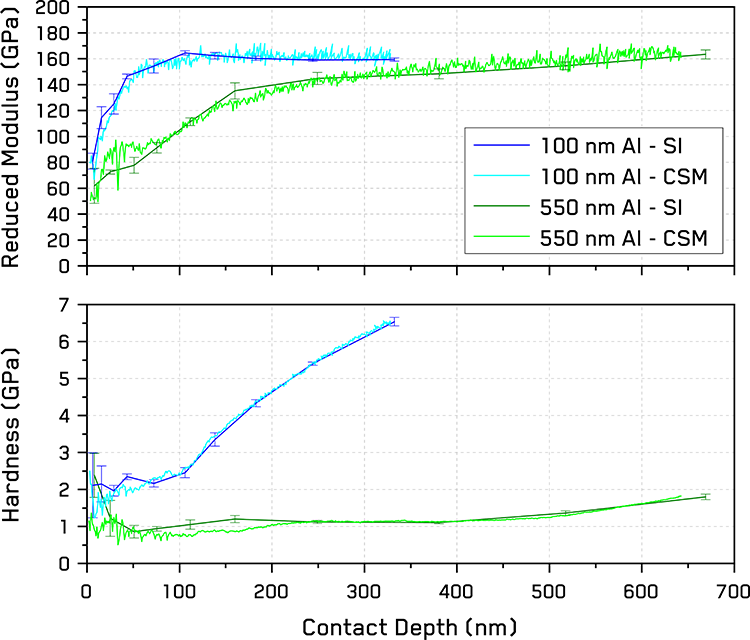
Figure 2. Simple indentation (SI) and continuous stiffness measurement (CSM) results for the 100 and 550 nm thick Aluminum films.
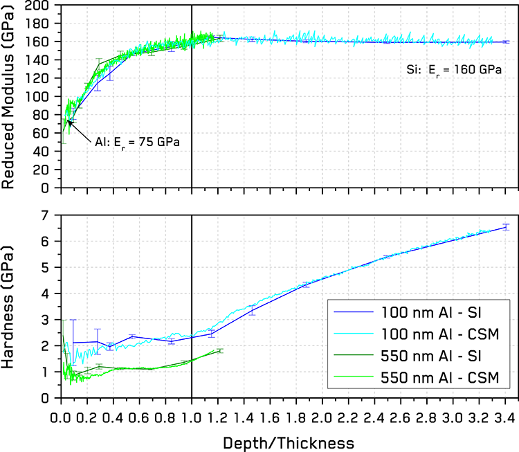
Figure 3. Simple indentation (SI) and continuous stiffness measurement (CSM) results as a function of normalized depth (Contact Depth/Film Thickness) for the 100 and 550 nm thick Aluminum films.
4. Conclusion
In this application note, nanoindentation testing in both SI and CSM modes were employed to evaluate the properties of two aluminum thin films with different thicknesses. Both simple and CSM modes were shown to yield similar values, but the CSM mode provides significantly more data in a much shorter time frame. Further, as CSM provides the same amount of information from a single indent, rather than 10s of indents, it allows coatings to be evaluated with much higher spatial resolution. Similar results were obtained on the coatings by both SI and CSM indentations. Reduced modulus results from the two coating thicknesses converged onto a single trend upon normalizing the results by depth/thickness ratio with both the coating and substrate moduli accurately determined. This successfully demonstrates the application of nanoindentation testing for the evaluation of thin films.
References
- T. Bell, A. Bendeli, J. Field, M. Swain, E. Thwaite. The determination of surface plastic and elastic properties by ultra
micro-indentation, Metrologia 28 (1991) 463.
- W.C. Oliver, G.M. Pharr. Measurement of hardness and elastic modulus by instrumented indentation: Advances in understanding and refinements to methodology, Journal of Materials Research 19 (2004) 3-20.
- ISO 14577-4. Metallic Materials—Instrumented Indentation Test for Hardness and Materials Parameters—Part 4: Test Method for Metallic and Non-metallic Coatings. International Organization for Standardization Winterthur, Switzerland, 2016.
- G.J.K. Schaffar, J. Kappacher, D. Tscharnuter, V. Maier-Kiener. The Phase Transformation of Silicon Assessed by an Unloading Contact Pressure Approach, JOM 74 (2022) 2220-2230.
- P. Filippov, U. Koch. Nanoindentation of Aluminum Single Crystals: Experimental Study on Influencing Factors, Materials 12 (2019) 3688.

