Thin films and coatings with thicknesses under 100 nm are an intrinsic part of modern technology, finding applications in semiconductors, optics, flexible electronics, and functionalized surfaces. To ensure full functionality in these coating systems, the coatings must be cohesive and well-adhered to their substrate, whether that is another coating, a silicon wafer, or precision optics. Nano-scratch testing provides a rapid, local method for investigating the mechanical behavior of thin films. For a system to perform this application, three factors are important to remember: high resolution sensing, lateral stiffness, and scanning actuation. In this application note, nano-scratch measurements are successfully demonstrated on two different thin films with thicknesses between 60-100 nm.
Introduction
Scratch testing is one of the simplest tests to investigate the mechanical behavior of coatings in shear loading. This provides a measurement of the adhesion, abrasion resistance or hardness, and integrity of a coating. At the micro-scale, scratch testing allows a semi-quantitative [1] analysis of a coating’s adhesion as defined in ASTM standard C1624-05 [2]. This specifies scratch testing at a constant speed with a Rockwell C diamond indenter (200 µm radius sphere with 120° included angle) with a defined normal force (constant or progressively increasing) for a defined distance and defines the forces at which specific types of damage occurs as critical loads, Lc. These are then used to determine the coating adhesion. An excellent atlas of the various types of coating damage and failure types can be found in the work of S.J. Bull [3]. However, this method is only valid for coatings between 0.1-30 µm in thickness, as smaller probe radii and different force levels are required for thin films on the nanometer scale.
As nanometer scale coatings are ubiquitous in many modern technologies, nano-scratch testing is an attractive method for assessing coating performance for research and development as well as quality assurance. Modified versions of the analysis in ASTM C1624-05 can be used with smaller spherical probe radii to provide a measure of coating adhesion, and sharper probes (Berkovich and Cube Corner) can be used to rank coating performance. In this application note, nano-scratch measurements are conducted on two different thin films illustrating both well-adhered and low coating adhesion behaviors.
Experimental Considerations
For a system to perform this application, three factors are important to remember: high resolution sensing, lateral stiffness, and scanning actuation. These factors are required to perform a scratch where the loading is smoothly applied during a linearly-scanning scratch to accurately determine the film’s behavior and failure with high depth and force resolution.
High Resolution Sensing
For clear resolution of the forces and displacements involved in nano-scale scratches, a sensor with the appropriate normal and lateral force resolution is critical to resolve the phenomenon and precisely measure the displacements involved. This is particularly important for surface profilometry with sharp probes. Systems must have low force resolution in order to perform low-load scans before and after scratch testing at higher loads.
Lateral Stiffness
As a scratch test is performed, the probe experiences both normal and lateral forces. If the system’s lateral stiffness is insufficient, a significant portion of the scratch’s specified length may be reduced due to elastic deflection of the probe laterally. Additionally, in the event of a fracture event, low lateral stiffness systems can experience sudden large, lateral displacement bursts as the elastic energy is released, preventing smooth performance of the test.
Scanning Actuation
To perform a scratch test, it is required to scan either the probe or the sample laterally relative to each other. This should be performed linearly with high positioning accuracy to ensure multi-pass testing is performed over the same line. This is best accomplished by scanning the sample relative to the indenter probe, as most actuators for scanning a probe across the surface induce some tilt or rotation of the probe along an arc, rather than purely linear motion. This changes the rake angle of the probe against the sample, changing the loading of the sample. Further, in order to meet the ASTM requirement of constant speed, a scratch should be performed smoothly with displacement control, so that any failures are not obscured by irregular or stick-slip motion.
Multi-pass Scratch Testing
A 3-pass procedure was used to perform scratch testing on the coating samples, as diagrammed in Figure 1. The 1st pass measures the initial surface topology using a normal force low enough to prevent plastic deformation but high enough to ensure good contact, in this case 25 µN. A small sample tilt is observed in the data, while the forces are small and constant. The 2nd pass performs the scratch using a ramped load profile where the load is progressively increased in a linear fashion to a specified maximum load (e.g. 5, 10 & 20 mN) to continuously investigate the coating performance. Pre- and post-scan regions of low-load scanning in the 2nd pass are included to profile any surface deformation in the scratch vicinity. Between these, the force is observed to progressively increase during scanning with the lateral force appearing smaller but proportional to the normal force, and the displacement increases proportionally as well with a negative bump at the end due to pile-up ahead of the scratch. Finally, a 3rd pass is performed at low normal force to measure the residual surface topology after the ramped-load scratch. This shows constant low forces again, except for a small perturbation as the probe encounters the pile-up ahead of the scratch trace. The displacements are significantly smaller than during the second pass due to elastic recovery, except for the pile-up, which was already unloaded during its profiling in the 2nd scan. Loaded and residual depths are determined by subtracting the initial displacement (1st pass) from the scratch (2nd pass) and final (3rd pass) displacements to determine the changes in the surface during and after the scratch.
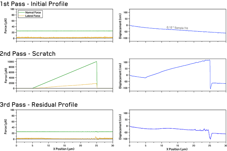 Figure 1. Illustration of a 3-pass scratch procedure showing the forces and displacements measured during the 1st initial profiling pass, the 2nd ramped-load scratch pass, and the 3rd residual surface profile pass.
Experimental Procedures
Coating samples were provided by SwissCluster AG (Thun, Switzerland). The alumina (Al2O3) coating was made via thermal atomic layer deposition (ALD) using a temperature gradient stage ranging from room temperature to 300 °C using trimethyl-aluminum Al(CH3)3, or TMA, kept at room temperature and DI water kept at room temperature. The deposition times consisted of 150 ms pulse of TMA and 300 ms pulse of H2O followed by a 10 s purging with argon after each pulse, which was continued until a thickness of ~100 nm was achieved. The TiN ALD coating was made via microwave plasma enhanced ALD (PE-ALD) at a substrate temperature of 200 °C using Tetrakis (dimethylamino) titanium (TDMAT) kept at 60 °C and N2 plasma as the second precursor using two microwave sources, each at 175W. The deposition times consisted of a 500 ms pulse of TDMAT and a 12 s pulse of N2 plasma with 10 sccm followed by a 10 s purge with argon after each pulse. A coating thickness of ~60 nm was achieved.
Scratch testing was performed using an NMT04 In-Situ SEM Nanoindenter with a FT-S20,000-2Axis sensor fitted with a Berkovich diamond with the facet edge oriented forward in the direction of scratch motion. To perform the scratch, the sample is moved relative to the indenter tip using the FT-SEM-ST04 scratch module’s independent piezo-scanner. Testing was performed in situ in a Zeiss EVO 25 SEM at an acceleration voltage of 10 kV. Electron micrographs were taken of each test region using an Everhard-Thornley detector for secondary electrons (SE) and a HD Backscattered Electron Detector (BSE).
Results and Discussion
Two different films were investigated in this application note. Key results from these tests are the measured displacements and forces during the scratch testing and the visualization of the residual scratches from either microscopy or topology characterization. It is very helpful to have a plurality of data from multiple modes to accurately identify critical loads for different failure modes.
Scratches performed on the ALD alumina sample (Figure 2) all show smooth, well-adhered behavior without any apparent adhesive failures. This type of scratch deformation is called ploughing. Loaded depths and forces smoothly increase during the ramp until the depth surpasses the coating thickness and encounters the silicon substrate. This can be seen in both SE and BSE micrographs as a slight change in contrast inside the scratch trace, which coincides with ripples in the pile-up. These ripples are also observed in the residual depth curve, which shows that an apparent plateau is achieved at a depth of 20 nm. However, this likely does not represent the maximum depth of the scratch trace, due to contact of the Berkovich indenter with the pile-up around the scratch.
The behavior of the ALD TiN film is much more brittle in comparison to the ALD alumina with a clear coating failure occurring during the scratch - Figure 3. This is clearly revealed in all measured signals except the applied normal load, which maintains a steady progressive increase without any deviations during the coating fractures. Over 6 scratches to a maximum load of 10 mN, this critical load was observed to occur consistently at Lc = 5.2 ± 0.2 mN.
At the critical load, the loaded depth is observed to deviate from smooth behavior and penetrate deeper than the previous trend, consistent with the fractured coating being less able to support the normal load. As the loaded depth increases, the contact area of the indenter also increases, so an increase in the lateral force is also noted. The deviation in the residual depth occurs at an X position slightly earlier than the critical load, due to the scanning probe encountering protruding debris from the fractured coating, which can be seen in the electron micrographs in Figure 3. This makes the residual depth less reliable for critical load determination due to probe radius effects. The failure mode of this coating occurs via a mixture of chipping and ploughing [3] due to the edge-forward orientation of the indenter.
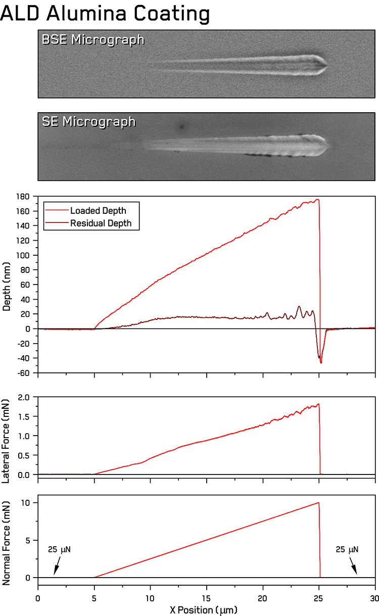
Figure 2. Scratch forces and depths vs. position during a 10 mN progressive scratch of 103 nm thick ALD alumina on Silicon with accompanying electron micrographs of the residual scratches.
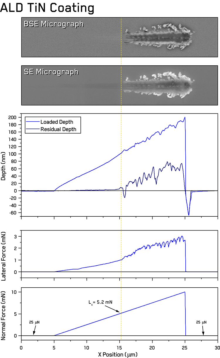
Figure 3. Scratch forces and depths vs. position during a 10 mN progressive scratch of 60 nm thick ALD TiN on Silicon with accompanying electron micrographs of the residual scratches and the critical load noted.
As mentioned in the procedure, ramped-load scratches were performed to several different maximum loads. Figures 2 and 3 were both performed to a maximum load of 10 mN. Figure 4 was performed to three different maximum loads over the same scratch distances: 5, 10, 20 mN. Residual depths are not shown in Figure 4 for clarity. The 10 mN curve is the same as Figure 3.
Despite the differences in maximum load and loading rate over distance, dL/dX, the critical loads occur at very similar normal loads. Lc is observed to slightly decrease with decreasing dL/dX, as is commonly observed [4]. This highlights the importance of keeping testing profiles (max. load, loading rate, scanning rate, etc.) identical for proper comparisons.
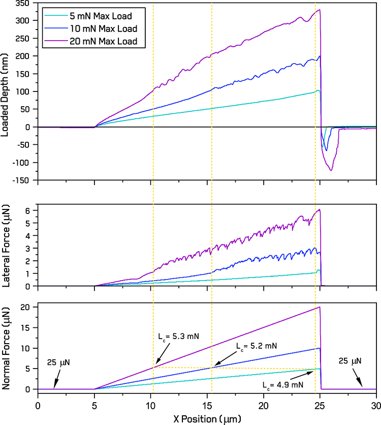 Figure 4. Scratch forces and loaded depth vs. position during progressive scratches to different maximum loads on 60 nm thick ALD alumina on Silicon with variation in critical load marked.
Conclusion
In this application note, nano-scratch testing was employed to evaluate the performance of ALD alumina and TiN coatings. Nano-scratch is an attractive technique for such measurements, as it allows local, rapid measurements on coatings with thicknesses in the nanometer scale. For semi-quantitative adhesion measurements, a sphero-conical probe is recommended. ALD alumina films showed strong adherence to the substrate and failed by ploughing in a ductile manner. ALD TiN films illustrated a chipping failure marked by a critical load of ~5.2 mN with a small dependence on the loading/scanning rate. This successfully demonstrates the application of nano-scratch testing for the evaluation of the performance and adhesion of coatings with thicknesses below 100 nm.
References
- S.J. Bull, E.G. Berasetegui. Tribol. Int. 39 (2006) 99-114.
- ASTM Standard C1624 (05)–Standard Test Method for Adhesion Strength and Mechanical Failure Modes of Ceramic Coatings by Quantitative Single Point Scratch testing, ASTM International (2005).
- S. Bull. Tribol. Int. 30 (1997) 491-498.
- B. Beake, A. Harris, T. Liskiewicz. Tribology-Materials, Surfaces & Interfaces 7 (2013) 87-96.

