Surface treatments, such as coatings, nitriding, and shot peening, are invaluable to industry as a method to improve the functional and mechanical behavior of parts without changing the primary material. Cross-sectional mechanical microscopy was performed on two different anodized coatings, hard anodized and plasma electrolytic oxidation, on a 5052 aluminum alloy. Mechanical microscopy reveals the presence of different layers within the two coatings with varying mechanical properties and densities while accurately determining the mechanical properties throughout. This is only possible using an indentation system with a combination of high positioning accuracy, speed, and sensitivity. The application of mechanical microscopy to surface treatments and coatings offers higher resolution characterization of both microstructure and mechanical properties than previously possible.
Introduction
Nanoindentation mapping is one of the best ways of investigating the local mechanical properties, i.e. hardness and elastic modulus [1], of complex microstructures. One application of this is using indentation mapping to quantify the mechanical property variation of surface treatments such as coatings, nitriding, shot peening, or radiation. Each of these methods can be used to modify the mechanical and/or tribochemical performance of surfaces. However, the mechanical behavior is often variable within coatings and with distance from the surface, requiring accurate characterization for both development and quality control. For example, many coating systems are not homogenous and have less dense, softer outer layers, or the hardness of nitrided surfaces usually varies with depth from the surface due to the diffusion kinetics of nitrogen.
An excellent way to investigate this is via a cross-section of the surface, rather than mechanically testing the surface in a top-down manner. This perspective allows the variation in properties as a function of distance from the top surface to be easily investigated both metallographically and mechanically. Metallographic investigation techniques, such as etching a polished cross-section to determine nitriding depth, are useful for determining diffusion rates and microstructure. However, mechanical methods are required to determine the effectiveness of surface treatments on enhancing the mechanical performance.
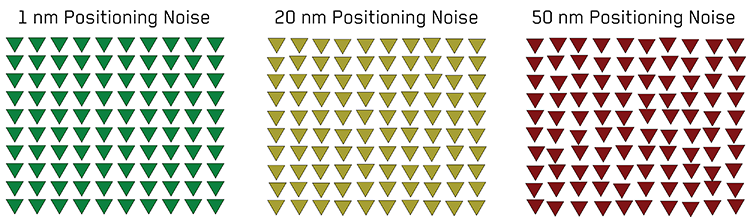 Figure 1. Overview of the experimental setup including a description of how the LED was connected to the Arduino, a general illustration of the input/output of the fiber optic cable, and Czerny-Turner geometry of the Kymera 193 spectrograph.
In this application note, cross-sectional nanoindentation mapping is used to investigate the mechanical performance of two different anodized coatings on aluminum: plasma electrolytic oxidation and conventional anodizing. These coatings have been previously investigated [2] using a range of microindentation and nanoindentation techniques in 2012. Indentation mapping is performed using regularly spaced and sized, nanoscale indentations performed at high-speed using continuous stiffness measurement to determine mechanical properties as a function of indentation depth at each location. This provides a high-resolution mechanical image of the microstructure that we at Oxford Instruments like to call Mechanical Microscopy.
Experimental Considerations
For a system to perform this application, several factors are important to consider: positioning, speed, and sensitivity. Regular and precise sample positioning is required to achieve a high-resolution grid of indentations. An image with differently-sized or
irregularly-spaced pixels is not ideal. This requires high precision positioning to achieve regular grids at small lateral spacings. Testing should be performed under displacement control, so that every indentation is made to the same maximum depth regardless
of the hardness of the material. The speed of indentation is important for high-resolution maps to be acquired in a reasonable amount of time. Lastly, the measurement sensitivity is extremely important, as a fast, large map is useless if the data is too noisy.
Positioning accuracy, displacement control, speed, and sensitivity are all vital to this application.
Positioning Requirements
In order to produce a regular map of mechanical properties, each datapoint should correspond to indentation of the same size. This allows the indentations to be regularly spaced without overlapping, achieving the maximum possible resolution for the
chosen step size. The recommended ratio for indentation depth, D, to the spacing, L, between Berkovich indentations is a factor of 10 to prevent neighboring indentations from influencing each other [3].
Sample Stage Positioning Noise
If one considers the sample stages’ positioning noise, to ensure 95% (2σ) of indentations meet the 10× criterion, the spacing should be: L = 10D+4σ, where σ is the standard deviation of the positioning noise floor. The extra 4σ is required to ensure that positioning noise from two neighboring indentations do not result in interactions due to indentations touching – as shown in Figure 1. This relationship scales, so indentation grids with smaller inter-indent spacings require higher precision, low noise positioning.
Displacement Control
However, positioning can only be made this finely and regular if the indentations are the same size, i.e. performed to the same depth. In load control, the load must be carefully chosen to ensure that the spacing is proportional to the indentation produced in the
softest phase in the map. Otherwise, indentations in the soft region will overlap with its neighbors. This means for indentations maps performed in load control, a significant disparity in indentations depths and spacings can be expected for maps over dissimilar
phases. This is shown in Figure 2, where the 20 mN indentations in the substrate are larger than in the coating (350 nm in HA vs 900nm in aluminum).
This can make it difficult to compare results from indentations in different phases due to additional differences due to indentation size effects. It also means that space in the mapping region is ‘wasted’ as the loaded areas and volumes are not consistent
between all the phases. In displacement control, indentations are all performed to the same maximum depth, ensuring similar indentation sizes and regular with minor variations from differences in elastic recovery. The elastic compliance of the load
cell forces is also important to minimize in displacement control, as the applied displacement will have elastic components from both the system and the sample.
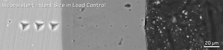 Figure 2. BSE micrograph of a line of 20 mN indentations across the HA coating illustrating the trade-off in spacing and depth in mapping performed under load control.
Speed
A typical, constant strain rate indentation may have a test duration of ~2 min, which means that a 100×100 map would require nearly two weeks of testing time. While this may be feasible, clearly there is a significant incentive to test at higher speeds. This has
led us to push the limits of the test speeds by using higher speed electronics and sample positioning stages. This has significantly decreased testing time, so that indentations can be performed in ~1 second. This 100× increase in testing rate allows a 100×100 map to be performed in hours instead of weeks.
Sensitivity
High speed, regular maps of indentations are not useful unless the measurement sensitivity is high enough to resolve the variations within the mapped region. The measurement sensitivity is a function of several parameters: force and displacement noise floors, system dynamics, repeatability.
The primary influence on system’s measurement sensitivity is its noise floor in both force and displacement. For performing nanoindentation maps with maximum depths of < 100 nm, tolerances in measurement noise must be very tight, particularly
for identifying the contact point and during CSM measurements. Misidentification of the contact point can easily impart significant error into an otherwise high-precision measurement, so high sampling rates with low noise are important. It is also important to
have access to the raw data to adjust the fitting parameters for contact point identification to achieve optimum settings for each material.
Continuous stiffness measurements (CSM) allow the acquisition of many stiffness measurements to be acquired as a function of penetration depth during a single indentation. These oscillations should ideally be small relative to the indentation force and depth in order to reduce any cyclic loading effects on the materials [4], which further increases the sensitivity requirements on performing CSM at depths of < 100 nm. However, in addition to the force and displacement noise floors, the system’s repeatability is also a critical factor. For this, a system should be free damping or hysteresis effects which may interfere with dynamic measurements.
Experimental Procedures
Two different coatings are investigated in this application note: one conventionally hard-anodized (HA) and one plasma electrolytic oxidation (PEO) coating. Hard anodized coatings were made using a sulfuric acid process following the Mil-8625, Type III
specification. PEO coatings were prepared by using 50 kW Keronite PEO equipment and a low-concentration electrolyte. Full details on coating manufacture can be found elsewhere [2]. Samples for indentation testing were sectioned and mounted in bakelite in
cross-section for metallographic preparation. The samples were then ground and polished using successively finer media to a final polish with 0.25 µm diamond paste.
Indentation maps were performed using a i04 Femto-Indenter with a 20 mN sensor fitted with a diamond Berkovich indenter tip. Indentation grids were performed with a 1 µm spacing and a 95 nm maximum indentation depth at a rate of ~2.5 s per indent. Grids of 100×150 or 150×150 indentations were made, depending on the coating thickness. Each indentation was made in displacement control to a target depth with continuous stiffness measurement with an oscillation amplitude of 4 nm. This provides
hardness and modulus as a function of depth, and representative mean values are taken from the final 25% of the maximum depth. Indentation maps of Backscattered electron (BSE) micrographs of the indentation regions were acquired using a Zeiss EVO 25 SEM at an acceleration voltage of 20 kV.
Results and Discussion
Before presenting the mechanical microscopy results, the electron micrographs of the coating cross-sections are presented to illustrate the coatings’ microstructures. Backscattered electron micrographs (Fig. 3) show the significant structural differences between these coatings. The aluminum alloy substrate is on the left side of the micrographs, and the bakelite mounting material is shown on the right side.
In both cases, the coatings display well-bonded coating–substrate interfaces without cracks or porosity. The hard anodized coating displays only large transverse cracks through the coating thickness along with some micro-porosity. However, the PEO coating (Fig. 4b) shows a finer structure at the coating surface.
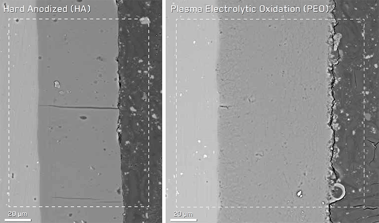
Figure 3. BSE micrographs of cross-sections of (a) hard anodized and (b) PEO coatings on AA5052 with the indentation mapping regions indicated by dashed rectangles. Indentations are sufficiently shallow ( ≤100 nm) to not significantly obscure the view of the microstructure.
This results from the high temperature plasma discharges, which are a feature of the PEO process that allows high temperature, harder phases to form. The PEO coating additionally shows an extensive micro-crack structure with a reticulated structure
near the coating–substrate interface giving way to a more layered appearance nearer the coating surface.
At first glance, a close correspondence between mechanical micrographs of the coating cross-sections shown in Figure 4 and the electron micro-graphs is easily observed – particularly in the overall morphology, transverse cracks, and large pores. However,
several microstructural features can be noted in the mechanical micrographs which were not easily observed in the electron micrographs. The HA coating shows a harder and stiffer layer near the aluminum interface, which presumably indicates a higher
density layer of amorphous alumina. This was also noted previously [2]; where small number of indents near the interface appeared harder, and a color change was observed near the substrate inthe ball-cratering impressions. Additional porosity is observable
in the mechanical micrographs, as is a decreasing gradient in hardness and reduced modulus it approaches the surface.
Significant differences are also notable in the PEO sample, where again significantly more porosity is resolved in the mechanical micrograph than the BSE micrograph. This corresponds well with the porosity and micro-crack network observed in the BSE micrograph, however the contrast observed in mechanical performance is much greater. Due to this greater contrast, the PEO coating can easily be seen to correspond to two different layers: a harder, denser inner layer and a porous outer layer.
In comparison to previous investigations [2], the peak reduced modulus values observed in Figure 4 are closer to expected values for fully dense amorphous (Er = 126 GPa [5]) and alpha alumina (Er = 350 GPa [6]) than previous measurements. This is consistent with the higher resolution measurements in the current work [95 nm depth/1 µm spacing) sampling more locally than previous indentations (750 nm depth/20 µm spacing), and thus being less influenced by porosity.
These new measurements also reveal the reason for the large degree of scatter in previous measurements on PEO coatings, as what could only be seen as scatter in the data before is now clearly resolved by mechanical microscopy as porosity and density variations. This is due to the vast numerical superiority of mechanical microscopy measurements, where 15,000 indentations were performed in the same total amount of time as the 100 indentations performed previously [2].
This is important to consider when examining the hardness results. On average, mechanical microscopy measures slightly higher hardness values than previous, due to its higher strain rates and smaller indentation sizes. Mean hardness values for the majority of the HA coating by mechanical microscopy were found to be ~6 GPa, while previous nanoindentation hardness was ~5 GPa. Knoop and Vickers hardness for the HA coating was ~5.5 and 5 GPa, respectively. In the PEO coating, mean hardness values
were observed to be ~16.5 GPa, while previous nanoindentation measurements were ~15.5 GPa. Knoop and Vickers hardness were both ~14 GPa. Despite different in scale of ~8×, current and previous nanoindentation results are quite consistent, as are the hardness results from the much larger Knoop and Vickers indentations.
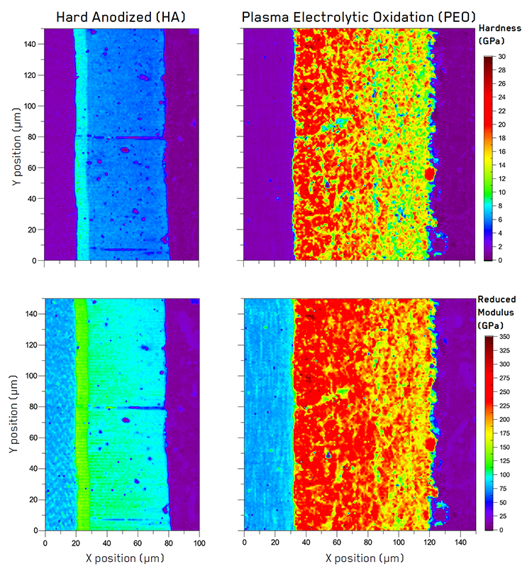
Figure 4. Mechanical microscopy maps of hardness and reduced modulus from the HA and PEO coatings with mechanical property values indicated by the color scales on the right.
Conclusion
Mechanical microscopy using high-speed nanoindentation has been demonstrated to be a powerful method for the cross-sectional characterization of surface treatments. This application shows that mechanical microscopy can provide similar microstructural characterisation capabilities to electron microscopy at the micro-scale. For density variations, such as the harder near-surface layers in both coatings and the cracks and porosity, mechanical microscopy is shown to provide superior contrast to electron microscopy. This is only possible through the combination of high positioning accuracy, displacement control, speed, and sensitivity of the indentation system. The PEO coating was revealed to be several times harder than the HA coating, and hardness values were consistent with previous measurements. Reduced modulus values showed peak values closer to their fully dense values than previous measurements, due to the increased spatial resolution of the current measurements.
References
- W.C. Oliver, G.M. Pharr, Journal of Materials Research, 7 (1992) 1564-1583.
- J.M. Wheeler, J.A. Curran, S. Shrestha, Surface and Coatings Technology, 207 (2012) 480-488.
- P.S. Phani, W. Oliver, Materials & Design, 164 (2019) 107563.
- M.J. Cordill, M.S. Lund, J. Parker, C. Leighton, A.K. Nair, D. Farkas, N.R. Moody, W.W. Gerberich, International Journal of Plasticity, 25 (2009) 2045-2058.
- A.N. Govyadinov, I.L. Grigorishin, P.P. Mardilovich, ITGFachbericht ‘Vacuum und Displays’, in, VDE, Berlin, 1995, pp. 161.
- J. Wachtman, W. Tefft, D. Lam, C. Apstein, Physical Review, 122 (1961) 1754-1759.

